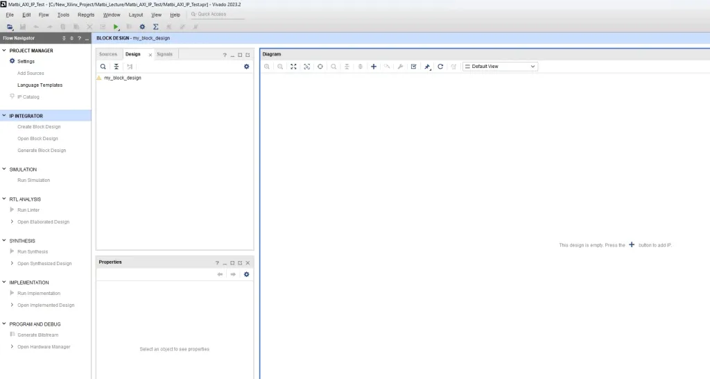
Click “Create Block Design” on the left “Flow Navigator” tab to create a Block Design.
2. Add ZYNQ PS and AXI IP to Block Design
Add “AXI4-Lite IP” and “ZYNQ7 PS” to Block Design, and Click “Run Connection Automation” after completing basic settings of ZYNQ7 PS, including DDR and UART.
When “Run Connection Automation” is completed, “FCLK_CLK0”, a clock generated by ZYNQ PS, is connected as follows.
① ZYNQ PS IP’s “M_AXI_GP0_ACLK”: The AXI interface provides the timing of all operations related to AXI data transmission based on the clock signal connected through the port. ② AXI4-Lite IP’s “s00_axi_aclk”: AXI4-Lite IP performs all operations related to AXI data transmission based on the clock signal connected through the port.
3. Add Integrated Logic Analyzer (ILA) for debugging AXI IP behavior
To verify that AXI IP is operating correctly, debug the AXI interface signal using ILA.
Right-click the AXI interface signal and click the “Debug” button as follows.
Then, you can see that bug shape appeared on the corresponding signal as follows, and Click the newly created “Run Connection Automation” button at the top.
When you click the “Run Connection Automation” button, a window related to the ILA setting appears as follows
In this example, you click ‘OK’ immediately without configuring anything else. The ILA helps to observe the actual signals of the connected ports based on the trigger conditions set by the user. (Therefore, the ILA is synthesized with the user’s design.)
Now, You can see that ILA has been added to Block Design.
Click “Optimize Routing”, “Regenerate Layout”, and “Validate Design” to optimize and validate the layout of Block Design.
4. Check the Address and Setting of AXI4-Lite IP
If you click “Address Editor” at the top, you can see that the AXI4-Lite IP is mapped to the Address (0x43C0_0000 to 0x43C0_FFFF) of the ZYNQ PS.
In fact, there are four registers used by the AXI IP, so the appropriate address range is “16” rather than “64K”. (Since one register → 32 bits → 4 Byte, four registers have 16 Byte, and because they are addressed in units of 1 Byte, the required address is “16”)
If you open the Address Map, you can see that it is mapped the same as the Address Range above.
The Base Address and Address Range can be changed by the user, in this example, only the Base Address is changed to “0x4000_0000” as a test. (You don’t have to change it.)
If you changed the settings, do “Optimize Routing”, “Regenerate Layout”, and “Validate Design” again.
5. Create an HDL Wrapper file for Block Design.
6. Create Bitstream and export Hardware Platform (XSA).
Let’s create a Bitstream of the design and check the implementation results.
The first red block is the resource occupied by the ILA, and the second red block is the resource occupied by the AXI4-Lite IP we created.
Our IP uses very little resources, but We can see that the ILA uses very many resources.
When Bitstream generation is completed, it is exported including Bitstream in the HW Platform.
7. Run Vitis and Create an SW Application project.
Create a Vitis Application project with the HW Platform (XSA) file generated by Vivado.
Looking at the left side of the generated Vitis project, it can be seen that the HW Platform contains device driver files.
If you look at the board support package (BSP) of the HW Platform, you can see that the driver file of the AXI4-Lite IP generated by Vivado has been created.
Xilinx kindly automatically creates driver files for custom AXI4-Lite IP.
8. Create code and Build project for register data Read / Write in AXI4-Lite IP
Write an example code for reading and writing data in the register of AXI4-Lite IP, and proceed the build as follows.
(Then, the error appears that there is no driver header file for the IP we generated, which is resolved by looking at the previous article)
When the output file is flashed to the board, You can see that the data is corecctly written/read in AXI IP as follows.
9. How to utilize ILA for debugging AXI interfaces
To observe this in more detail, let’s use Vivado’s ILA.
When you press “Open Hardware Manager” in Vivado, the ILA screen appears immediately.
Now, Set the trigger conditions for the ILA.
For Write operation, AXI4-Lite writes Data when both the Valid signal and the Ready signal become 1.
Therefore, set the values for both trigger items to 1,
Set the two trigger conditions to be triggered when the AND result is 1.
When all trigger conditions are set, click the “Run trigger for this ILA core” button.
Then, as follows, we can see the waveform when trigger conditions occur in the process of actually transmitting and receiving AXI interface signals between the board’s ZYNQ PS and AXI4-Lite IP.