Design the “BRAM Controller” module to Write/Read data to/from “BRAM”.
Attach an AXI4 Lite Interface to the “BRAM Controller” to create the “BRAM Controller AXI IP”.
Create a Vivado project to test the “BRAM Controller AXI IP” : Configure the ZYNQ PS, connect the BRAM Controller AXI IP, generate the Bitstream, and export the HW Platform (XSA).
Create a Vitis project based on the exported XSA file to Write/Read data to/from the “BRAM Controller AXI IP” in the ZYNQ PS.
Perform the basic setup for the Vitis project : Organize the ZYNQ PS folder structure and add common drivers (gpio, tim, gic, tft_lcd, and user_app). Add the driver paths to the arm gcc compiler/Linker (refer to Vitis Project Initial Setup).
Check the BSP for the HW Platform (XSA) to get the IP information (IP Base Address, Register Offset, and Register Write/Read Macro function).
Design the User IP Driver based on the above IP information.
Use the User IP Driver to design the IP test code and perform verification of the IP.
1. Design the BRAM module
The BRAM module can be designed as follows.
This BRAM is a Dual Port BRAM module but is configured to be used only as a Single Port.
To explain in detail,
Based on the parameter settings of “DWIDTH”, “AWIDTH”, and “MEM_SIZE”, you can determine the number of addresses that can be written/read and the number of data bits that one address can indicate.
These parameters can be reconfigured by the top module that instantiates this BRAM module.
Lastly, the statement “(* ram_style = ‘block’ *)” must be added before the reg variable so that the reg variable is allocated as BRAM.
2. Design the BRAM Controller module
When designing an IP, the most important thing is to clearly describe the behavior of the IP.
Additionally, creating a Timing Diagram is the most intuitive and useful method for describing the behavior of the IP.
“Timing Diagram” of BRAM Controller module
“Port & variable” of BRAM Controller module
“State Machine” of BRAM Controller module
“Behavior Description” Example of BRAM Controller module
“Simulation” of BRAM Controller module
Based on the Timing Diagram, write the TestBench code for the BRAM Controller and verify that the results are consistent using Vivado Simulation.
3. Create the BRAM Controller AXI IP
The basic procedure for creating any AXI IP can be followed by referring to the document “Creating a Custom AXI4-Lite IP“.
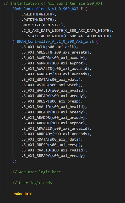
It is important to know how to connect the BRAM Controller to the AXI Bus Interface.
Here is the AXI Bus Interface code for this purpose:
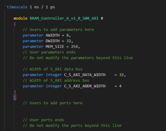
“BRAM_Controller_A_v1_0_S00_AXI”
① Parameter & Input/Output Port Definition of “BRAM_Controller_A_v1_0_S00_AXI”
The “BRAM Controller” communicates exclusively with the “ZYNQ PS” via the AXI Bus, so there is no need to define additional User Input/Output Ports. (If it needs to be connected to other modules or external pins besides the “ZYNQ PS,” then port definitions are required.)
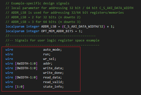
② Internal Wire Definition of “BRAM_Controller_A_v1_0_S00_AXI”
Create wire variables to connect the AXI Bus Register and the ports of the “BRAM Controller” instance.
③ Register’s Read-only Setting of “BRAM_Controller_A_v1_0_S00_AXI”
Among the AXI Bus Registers, there will be registers connected to the output signals of the FPGA (PL) module, storing the corresponding values. However, if the ZYNQ PS tries to store different data in these registers, a conflict (short circuit) may occur, potentially damaging the FPGA (PL).
(For example, if the output signal value ‘0’ from the FPGA module is connected to bit 1 of slv_reg1, and the ZYNQ PS tries to write ‘1’ to that bit of the register, a short circuit may occur, leading to FPGA (PL) damage.)
Therefore, registers connected to the outputs of the FPGA (PL) module should be considered Read-only Registers. The code should be modified to prevent write operations to these registers via the AXI Bus.
(Note : BRAM Controller Register Map)
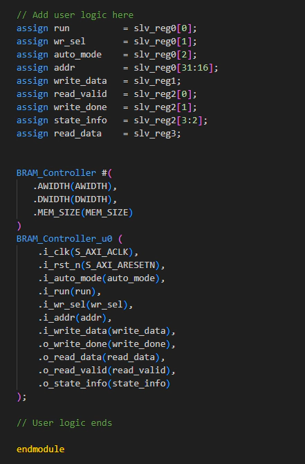
④ Connect Registers to “BRAM Controller” Instance’s Port via Wire
Using the wire variables created earlier, connect the AXI Bus Registers to the ports of the “BRAM Controller” instance.
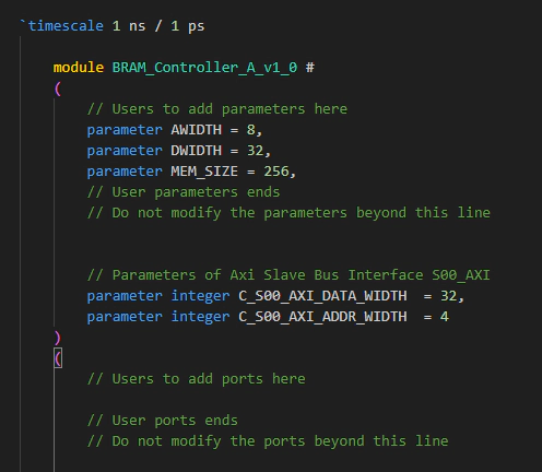
“BRAM_Controller_A_v1_0”
① Parameter & Input/Output Port Definition of “BRAM_Controller_A_v1_0”
Just like “BRAM_Controller_A_v1_0_S00_AXI,” the “BRAM Controller” communicates exclusively with the “ZYNQ PS” via the AXI Bus. Therefore, no additional User Input/Output Ports need to be defined.
② Add & Map Parameter, Input/Output Port of “BRAM_Controller_A_v1_0_S00_AXI” Instance
Since no separate User Input/Output Ports are defined and only parameters are added in “BRAM_Controller_A_v1_0_S00_AXI,” add the parameters as follows.
4. Create and Set up a Vivado Project to Test the BRAM Controller AXI IP
Now, to test the BRAM Controller AXI IP, create a separate Vivado project. In the Block Design, add the ZYNQ PS and the BRAM Controller AXI IP as follows.
Block Design of “BRAM Controller AXI IP” Test Vivado Project
Refer to the following for the ZYNQ PS configuration.
1. Configuring Quad SPI Flash in ZYNQ PS
① Configure the Peripheral I/O Pins for Flash Memory Connected to ZYNQ PS
The Quad SPI Flash Memory is dedicated to MIO1~6.
② The clock speed of the QSPI is set to 133MHz (based on the Winbond W25Q128JVEIQ product).
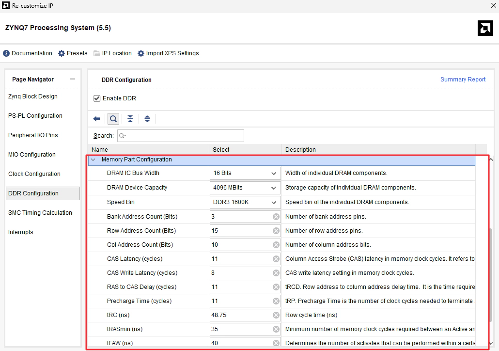
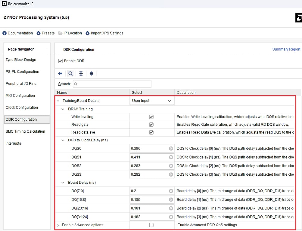
2. DDR Memory Configuration
① DDR Controller Configuration
The DDR controller of the ZYNQ PS supports various DDR memory types, so it must be configured according to the specifications of the DDR memory on the user’s board
Memory Type: DDR3 (Low Voltage)
Memory Part: Custom
② Memory Part Configuration
Based on the datasheet of the DDR memory on the user’s board, configure it as follows (based on Micron’s MT41K256M16TW-107 IT)
③ Training/Board Details
Based on the PCB artwork of the board, configure the delay values as follows.
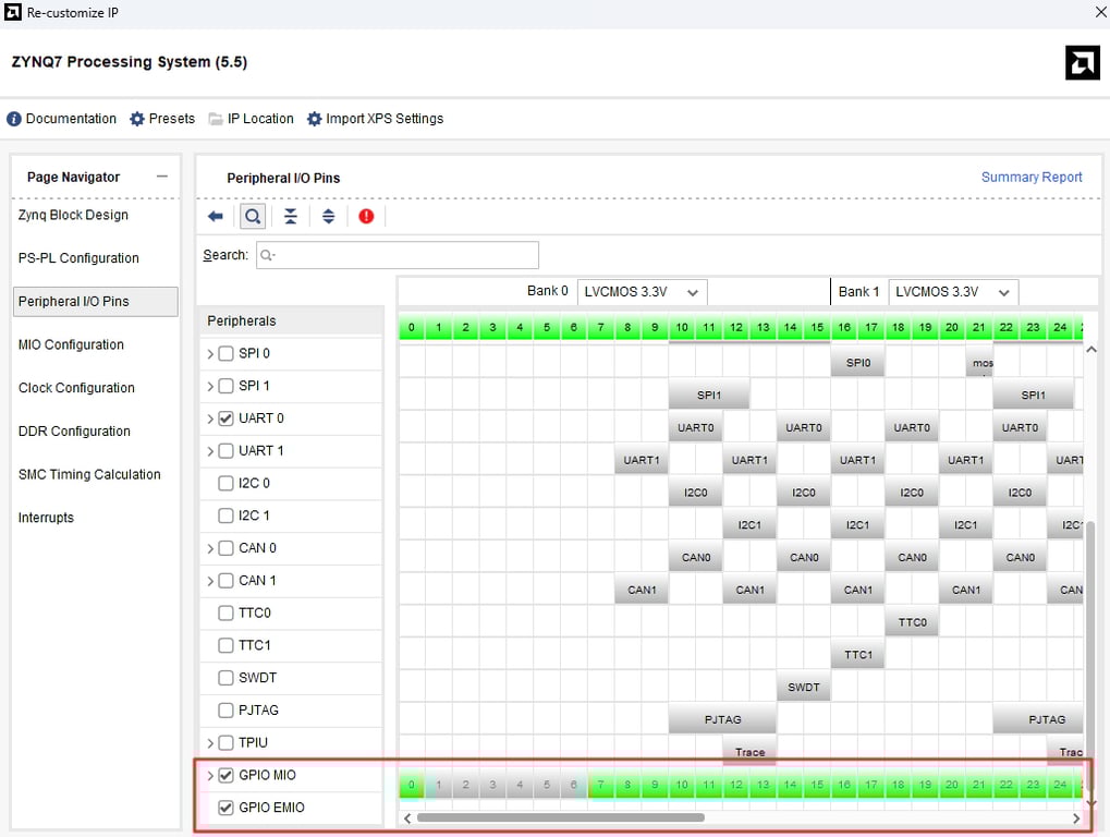
3. GPIO & EMIO Configuration
Enable the GPIO MIO and EMIO of the ZYNQ PS. (Although it is not strictly necessary for testing the BRAM Controller AXI IP, I usually enable it by default.)
GPIO MIO is uniquely assigned to pins in Bank 500/501 of the ZYNQ, but for EMIO, since it can be assigned to any PL pin desired by the user, the signal and pin assignments must be defined in the constraint file.
The currently used ‘ZYNQ-7Z010 SOM B’d (Rev.A)’ is connected to 15 peripherals including LEDs, switches, and a buzzer through PL pins. To control these from the ZYNQ PS, assign 15 EMIOs to the respective PL pins in the constraint file.
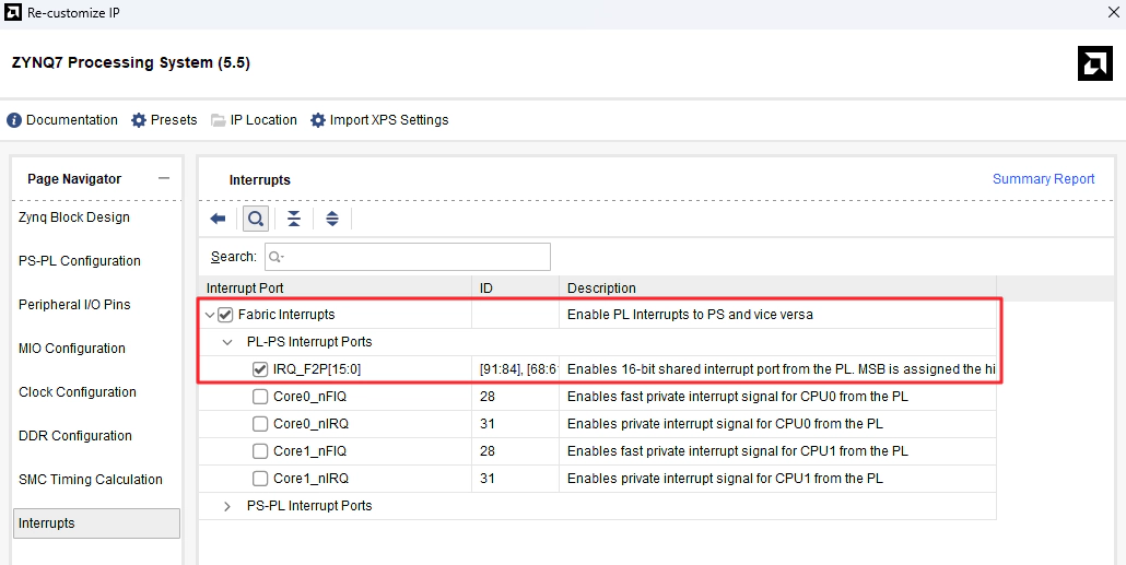
4. PL to PS Interrupt Configuration
Enable ‘PL to PS Interrupt’ to receive interrupts from the Tact switch configured via EMIO.
Add the ZYNQ PS and BRAM Controller AXI IP to the Block Design. Once the configuration of the ZYNQ PS is complete, generate the bitstream and export the hardware platform (XSA).
5~6. Create and configure a Vitis project for testing the BRAM Controller AXI IP
To test the ‘BRAM Controller AXI IP,’ data must be written to and read from the IP using the ZYNQ PS.
Therefore, create a Vitis project based on the HW Platform (XSA) file exported from Vivado and proceed with the basic project configuration (‘Vitis project initial setup‘).
→ Organize the folder structure for the ZYNQ PS and add the common drivers.
Structure of Vitis Project
7. Check the information about the IP in the BSP included in the HW Platform (XSA)
In the BSP’s ‘xparameters.h’, you can find the address information of the ‘BRAM Controller_A’ AXI IP. In ‘BRAM_Controller_A.h’, you can find the register offset information and basic register write/read functions for the ‘BRAM Controller’ AXI IP.
“xparameters.h”
“BRAM_Controller_A.h” (Header file of the Xilinx-generated IP)
8. Design the User IP Driver based on the IP information from the BSP
Based on the IP information from the BSP generated by Xilinx, design User IP Driver APIs to facilitate the use of the IP.
“ip_bram_ctrl_driver.h / ip_bram_ctrl_driver.c” (User IP Driver)
9. Design IP verification code using the User IP Driver and proceed with the verification of the IP
Write the IP verification code as follows and verify the IP.